- 您现在的位置:买卖IC网 > Sheet目录509 > SI4398DY-T1-GE3 (Vishay Siliconix)MOSFET N-CH 20V 19A 8-SOIC
Si4398DY
Vishay Siliconix
SPECIFICATIONS (T J = 25 °C, unless otherwise noted)
Parameter
Symbol
Test Conditions
Min.
Typ.
Max.
Unit
Static
Gate Threshold Voltage
V GS(th)
V DS = V GS , I D = 250 μA
1.0
3.0
V
Gate-Body Leakage
Zero Gate Voltage Drain Current
On-State Drain Current a
I GSS
I DSS
I D(on)
V DS = 0 V, V GS = ± 12 V
V DS = 20 V, V GS = 0 V
V DS = 20 V, V GS = 0 V, T J = 55 °C
V DS ≥ 5 V, V GS = 10 V
50
± 100
1
5
nA
μA
A
Drain-Source On-State Resistance a
Forward Transconductance a
Diode Forward Voltage a
R DS(on)
g fs
V SD
V GS = 10 V, I D = 25 A
V GS = 4.5 V, I D = 22 A
V DS = 10 V, I D = 15 A
I S = 2.9 A, V GS = 0 V
0.0023
0.0033
95
0.72
0.0028
0.0040
1.1
Ω
S
V
Dynamic b
Input Capacitance
C iss
5620
Output Capacitance
Reverse Transfer Capacitance
Total Gate Charge
Gate-Source Charge
Gate-Drain Charge
C oss
C rss
Q g
Q gs
Q gd
V DS = 10 V, V GS = 0 V, f = 1 MHz
V DS = 10 V, V GS = 4.5 V, I D = 20 A
1340
540
34
17.5
7.5
50
pF
nC
Gate Resistance
Turn-On Delay Time
Rise Time
Turn-Off Delay Time
Fall Time
Source-Drain Reverse Recovery Time
R g
t d(on)
t r
t d(off)
t f
t rr
V DD = 10 V, R L = 10 Ω
I D ? 1 A, V GEN = 4.5 V, R g = 6 Ω
I F = 2.9 A, dI/dt = 100 A/μs
0.7
1.4
23
15
80
23
50
2.1
35
23
120
35
80
Ω
ns
Notes:
a. Pulse test; pulse width ≤ 300 μs, duty cycle ≤ 2 %.
b. Guaranteed by design, not subject to production testing.
Stresses beyond those listed under “Absolute Maximum Ratings” may cause permanent damage to the device. These are stress ratings only, and functional operation
of the device at these or any other conditions beyond those indicated in the operational sections of the specifications is not implied. Exposure to absolute maximum
rating conditions for extended periods may affect device reliability.
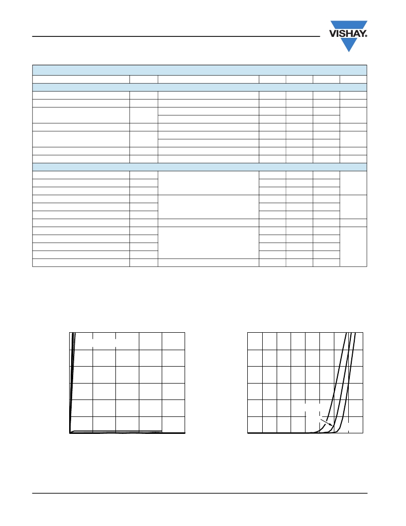
TYPICAL CHARACTERISTICS (25 °C, unless otherwise noted)
60
50
40
30
20
V GS = 10 V thr u 4 V
60
50
40
30
20
T C = 125 °C
10
0
10
0
25 °C
- 55 °C
0
1
2
3
4
5
0.0
0.5
1.0
1.5
2.0
2.5
3.0
3.5
4.0
www.vishay.com
2
V DS - Drain-to-So u rce V oltage ( V )
Output Characteristics
V GS - Gate-to-So u rce V oltage ( V )
Transfer Characteristics
Document Number: 73018
S11-0209-Rev. C, 14-Feb-11
发布紧急采购,3分钟左右您将得到回复。
相关PDF资料
SI4404DY-T1-GE3
MOSFET N-CH D-S 30V 8-SOIC
SI4406DY-T1-GE3
MOSFET N-CH D-S 30V 8-SOIC
SI4410DY
MOSFET N-CH 30V 10A 8-SOIC
SI4411DY-T1-GE3
MOSFET P-CH D-S 30V 8-SOIC
SI4420-D1-FT
IC TXRX FSK 915MHZ 5.4V 16-TSSOP
SI4420DYTR
MOSFET N-CH 30V 12.5A 8-SOIC
SI4421DY-T1-GE3
MOSFET P-CH D-S 20V 8-SOIC
SI4427BDY-T1-GE3
MOSFET P-CH 30V 9.7A 8SOIC
相关代理商/技术参数
SI43A
制造商:未知厂家 制造商全称:未知厂家 功能描述:SMT Power Inductor
SI4401BDY
制造商:VISHAY 制造商全称:Vishay Siliconix 功能描述:P-Channel 40-V (D-S) MOSFET
SI4401BDY_13
制造商:VISHAY 制造商全称:Vishay Siliconix 功能描述:P-Channel 40-V (D-S) MOSFET
SI4401BDY-E3
制造商:Vishay Intertechnologies 功能描述:Trans MOSFET P-CH 40V 8.7A 8-Pin SOIC N
SI4401BDY-T1-E3
功能描述:MOSFET 40V 10.5A 0.014Ohm RoHS:否 制造商:STMicroelectronics 晶体管极性:N-Channel 汲极/源极击穿电压:650 V 闸/源击穿电压:25 V 漏极连续电流:130 A 电阻汲极/源极 RDS(导通):0.014 Ohms 配置:Single 最大工作温度: 安装风格:Through Hole 封装 / 箱体:Max247 封装:Tube
SI4401BDY-T1-GE3
功能描述:MOSFET 40V 10.5A 2.9W 14mohm @ 10V RoHS:否 制造商:STMicroelectronics 晶体管极性:N-Channel 汲极/源极击穿电压:650 V 闸/源击穿电压:25 V 漏极连续电流:130 A 电阻汲极/源极 RDS(导通):0.014 Ohms 配置:Single 最大工作温度: 安装风格:Through Hole 封装 / 箱体:Max247 封装:Tube
SI4401BDY-T1-GE3
制造商:Vishay Siliconix 功能描述:P CHANNEL MOSFET -40V 10.5A SOIC 制造商:Vishay Siliconix 功能描述:P CHANNEL MOSFET, -40V, 10.5A, SOIC
SI4401DDY
制造商:VISHAY 制造商全称:Vishay Siliconix 功能描述:P-Channel 40 V (D-S) MOSFET
